- Home
- About Us
- Products
- High Purity Stainless Steel Tube/Pipe [11]
- Electro Polished Stainess Steel Tube / Pipe
- Stainless Steel Bright Annealed Tube / Pipe
- Cold Forged Bright Annealed Stainless Steel Tubing
- Sanitary Stainless Steel Tube / Pipe
- Bright Annealed Semi Seamless Stainless Steel Tube / Pipe (Seam Integrated Tubes)
- BA/EP Coiled Stainless Steel Tubing, Level Wound Coil Stainless Steel Tubing, Seamless Coil Tubing / Kuze Standard, Handy Tube Standard
- Heat Exchanger Stainless Steel Tubing
- High Purity Gas Fittings, Swagelok Parker, Stainless Steel Ultra High purity Fittings
- Gas Delivery Product, High Purity Gas Delivery Tube Assembly
- Kuze BA/EP Stainess Steel Tube / Pipe
- Cylinder Stainless Steel Tube, Pneumatic Cylinder Stainless Steel Tube, Air Cylinder Tube/ Pipe
- Bellows / Super Bellows / Vacuum Bellows [20]
- Super Bellows, Super Vacuum Bellows
- Vacuum Bellows, Super Bellows
- Vacuum Flexible Hose, Vacuum Metal Hose
- KF Vacuum Bellows, KF Flexible Hose, KF Flexible Metal Hose
- ISO Bellows, Vacuum Bellows, Flexible Hose, Flexible Metal Hose
- CF Bellows,Vacuum Bellows, Hydroformed Bellows,Flexible Hose,Metal Hose
- Seamless Metal Bellows, Seamless Stainless Steel Bellows
- Edge Welded Bellows, Welded Bellows
- Teflon Bellows, Ptfe Flexible Tube, Pfa Flexible Hose
- Flexible Metal Tubing, Formed Bellows
- Bellows Feedthrough, Bellows Seal, Formed Bellows Actuator Seal
- Formed Bellows, Hydro Formed Bellows 成型波紋管
- Expansion Joint, Bellows Expansion Joint, Metal Hose, Stainless Steel Flexible Tubing
- Metal Bellows
- Vacuum Flexible Tubing, Metal Hose Swagelok, Flexible Stainless Steel Hose
- Welded Bellows, Edge Welded Bellows, Welded Metal Bellows)
- Exhaust Gas Recirculation Tube, EGR Stainless Steel Tube, EGR pipe
- Turbo Charger Oil Drain Tube, Detroit Diesel Turbo Charger Oil Drain Pipe, Detroit Diesel Flex Stainless Steel Pipe,
- Secondary Air Injection Tube, AI Stainless Steel Tube, Air Injection Stainless Steel Pipe
- Turbo Oil Feed Tube, Turbo Charger Oil Feed Line, Detroit Diesel Flex Stainless Steel Pipe,
- Vacuum Components [61]
- Stainless Steel Bellows
- Super Bellows
- Vacuum Flexible Tubing, Stainless Steel Vacuum Flexible Hose, Vacuum Metal Hose
- Stainless Steel KF Vacuum Bellows, Flexible Hose,Flexible Metal Hose
- Stainless Steel ISO Bellows, Vacuum Bellows, Vacuum Flexible Tubing , Flexible Metal Hose
- Stainless Steel CF Bellows,Vacuum Bellows, Hydroformed Bellows,Flexible Hose,Metal Hose
- Stainless Steel Flexible Tubing, Formed Bellows
- Vacuum Bellows, Welded Bellows
- Seamless Metal Bellows
- Bellows Couplings, Flexible Bellows Couplings, Shaft Bellows Couplings
- Vacuum Angle Valves, Vacuum Bellows valves, Bellows Sealed Vacuum Valves
- Vacuum Valves, High Vacuum Valves, Vacuum Right Angle Valve, Vacuum Poppet Valve
- Vacuum Viewports, Vacuum Sight Glass
- Ferrofluid Seals, Magnetic Fluid Rotary Feedthroughs
- Stainless Steel Tube Fittings, High Purity Tube Fittings,SWG Instrumentation Fittings
- Feedthroughs, Vacuum Feedthroughs, Vacuum Rotary Feedthroughs
- BA Fittings, EP Fittings
- Vacuum Components, High Vacuum Components, Ultra High Vacuum Components
- Vacuum Components, Stainless Steel Vacuum Fittings, Custom Vacuum Components
- KF Fittings, KF Vacuum Fittings, KF Vacuum Flanges, Kwik Vacuum Flanges
- Vacuum Clamp, KF Clamp, Bulkhead Clamps
- Stainless Steel CF Vacuum Flanges, High Vacuum Flanges
- Stainless Steel CF Vacuum Flanges, High Vacuum Flanges
- ISO Vacuum Flange
- Stainless Steel KF Centering Ring, Mesh Centering Ring
- Stainless Steel ISO, KF Vacuum Centering Ring
- Stainless Steel CF Flange Tubing
- Vacuum Nipples, Vacuum Spool,ISO Vacuum Tubing Adaptor
- Stainless Steel Ultra High Vacuum tubing
- Vacuum Chamber
- Custom Vacuum Components, Custom Vacuum Fittings, Prefabricated Piping
- Vacuum Gate Valves, High Vacuum Gate Valve, Vacuum Bellows valves
- Orbit Welding Flange, Auto Welding Flange, Orbital Welding Flange
- Vacuum Traps, Vacuum Foreline Traps, Vacuum Filter
- Vacuum Quick Disconnect, Vacuum Gauge Seal Port, Vacuum Quick Connector
- Up To Air Valve, Vacuum Breaker Valve, Vacuum Leak Port
- Vacuum Hybrid Adapter, Vacuum fitting To Flanges
- Vacuum Ball Valve
- Vacuum Diaphragm Valve
- Vacuum Butterfly Valve
- Vacuum Check Valve, Vacuum Non Return Valve, Stainless Steel Vacuum Check Valve
- Vacuum Fittings, High Vacuum Fittings, Stainless Steel Vacuum Fittings, Custom Vacuum Components
- VCR Fittings, VCR Metal Gasket Seal Fittings, VCR Micro Fittings
- Vacuum Stainless Steel Clamp, KF Hinged Clamp, Bulkhead Clamps
- Ultra High Vacuum Parts, UHV Parts, HV Parts
- Ultra High Vacuum Products, UHV Products, HV Products
- Ultra High Vacuum Bellows, UHV Bellows, HV Bellows
- Ultra High Vacuum fittings
- Ultra High Vacuum Flanges, CF Vacuum Flanges
- High Vacuum Flanges, ISO Vacuum Flanges
- KF Vacuum Flanges, ISO KF Vacuum Flanges
- Ultra High Vacuum Components
- VG Vacuum Flanges, VF Vacuum Flanges, ASA Vacuum Flanges
- Ultra High Vacuum Valves, UHV Valves, High Vacuum Valves
- CF Vacuum Fittings, Ultra High Vacuum fittings
- ISO Vacuum Fittings, ISO Vacuum Flanges
- NW Fittings, NW Vacuum Fittings, NW Vacuum Flanges, Kwik Vacuum Flanges
- Stainless Steel Valve Components, Custom Valve Components
- ASA Vacuum Flanges, High Vacuum Flanges
- High Vacuum Bellows, UHV Bellows, Stainless Steel Bellows
- Camlock Couplings, Pixon Camlock Fittings, Camlock Quick Disconnect Couplings
- InP Wafer [8]
- ASME BPE Biopharm [33]
- Aseptic Diaphragm Valve
- Sanitary Aseptic Pneumatic Diaphragm Valve
- Sanitary Aseptic Diaphragm Valve
- Sanitary Aseptic Tank Bottom Diaphragm Valve
- Aseptic 3 way Diaphragm Valve
- Aseptic Bellows Diaphragm Valve
- Sanitary Bellows Valve
- Sanitary Check Valve, Hygienic Non Return Valve
- Air Blow Check Valve/Sanitary Air Blow Valve/3A Waukesha
- Air Vent Valve /Sanitary Air Relief Valve/3A Waukesha
- Sanitary Strainer, Sanitary Filter
- Aseptic Air Vent Filter, Millipore CWVT L10 01
- Rotary Spray Ball, Rotary Spray Head, Static Spray Ball
- Sanitary Sight Glass, Vacuum Viewport
- Sanitary Food Grade Hose, Sanitary flexible Hose
- Sanitary Pressure Gauge / Wika
- BA Fittings,EP Fittings
- BA Fittings, MP Fittings
- Tri - Clamp Fitting 3A
- Orbital(Automatic) Welding Tube Fittings
- Air Vent Valve
- High Vacuum Fittings, Stainless Steel Orbital(Automatic) Welding Tube Fitting
- Sanitary Cap 16W, Tube End Cap
- Stub End, Lap Joint, Stainless Steel Stub End
- Sanitary Stub End 14VB, Sanitary Lap Joint
- Vent Port Assembly, Spinner Flask Accessory
- Large Diameter Hygienic Diaphragm Valve
- Hygienic Relief Valve, Sanitary Safety Valve, Pressure Relief Valve
- Aseptic Sampling Valve, Hygienic Sampling Valve, Harvesting Valve
- Custom Sanitary Fittings, Prefabricated Piping
- Sanitary Mix Proof Double Seat Valve, Mix Proof Valve/Double Seat Valve
- Static Mixer, Sanitary Static Mixer / Noritake Type
- Large Diameter Hygienic Butterfly Valve
- High Purity Stainless Steel Tube/Pipe [11]
- News
- Manufacturing Process
- InP Wafer Technology
- Contact Us
Product
InP Wafer, InP Substrate
Product ID: InP substrate / InP substrate wafers
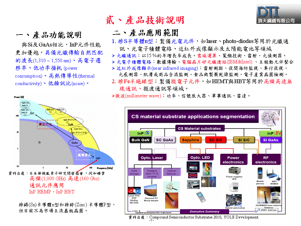
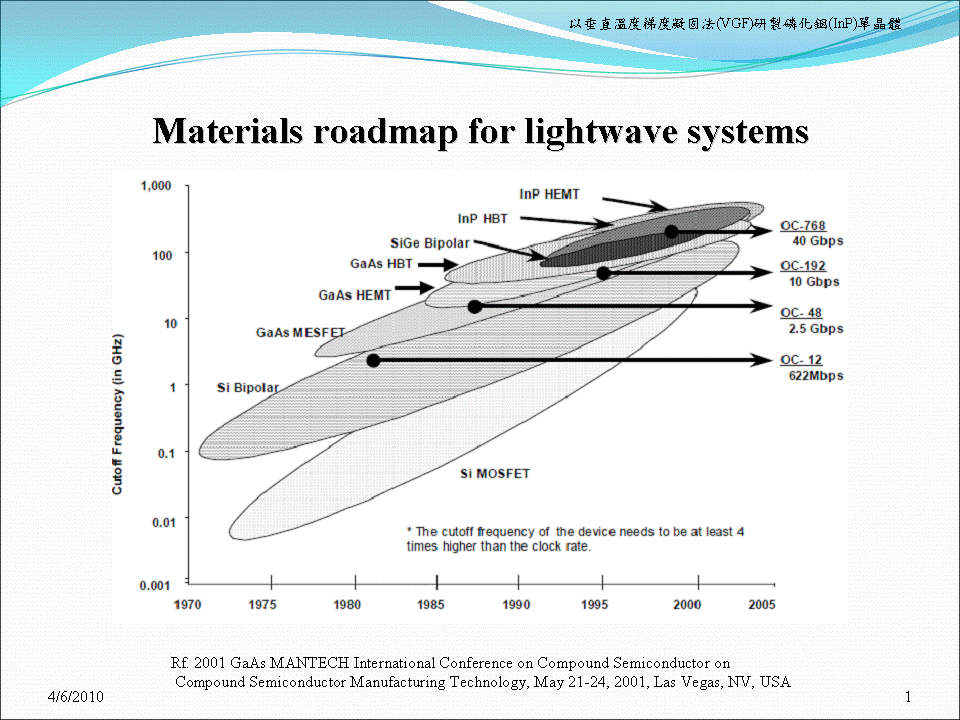
- Indium Phosphide and Related Materials-1
- Indium Phosphide and Related Materials-2
*Wafer Specifications&Test Report
Land Mark InP Test

|
Order Information:
- Minimum Order: Negotiable
- Branded Product