- Home
- About Us
- Products
- High Purity Stainless Steel Tube/Pipe [10]
- Electro Polished Stainess Steel Tube / Pipe
- Stainless Steel Bright Annealed Tube / Pipe
- DTI Cold Forged Bright Annealed Stainless Steel Tubing
- Sanitary Stainless Steel Tube / Pipe
- Bright Annealed Semi Seamless Stainless Steel Tube / Pipe (Seam Integrated Tubes)
- BA/EP Coiled Stainless Steel Tubing/Seamless Coil Tubing / Kuze Standard
- Heat Exchanger Stainless Steel Tubing
- High Purity Gas Fittings/Swagelok Parker Stainless Steel Ultra High purity Fittings
- Gas Delivery Product / High Purity Gas Delivery Tube Assembly
- Kuze BA/EP Stainess Steel Tube / Pipe
- Bellows / Super Bellows / Vacuum Bellows [15]
- Super Bellows/ Super Vacuum Bellows
- Vacuum Bellows/Super Bellows
- Vacuum Flexible Hose/ Vacuum Hose
- KF Vacuum Bellows, Flexible Hose/ Flexible Metal Hose
- ISO Bellows, Vacuum Bellows, Flexible Hose, Flexible Metal Hose
- CF Bellows,Vacuum Bellows, Hydroformed Bellows,Flexible Hose,Metal Hose
- Seamless Metal Bellows / Seamless Stainless Steel Bellows
- Edged Welded Bellows / Welded Bellows
- Teflon Bellows / Ptfe Flexible Tube / Pfa Flexible Hose
- Flexible Tubing/ Formed Bellows
- Bellows Feedthrough/Bellows Seal/Formed Bellows Actuator Seal
- Formed Bellows/Hydro Formed Bellows 成型波紋管
- Expansion Joint/Bellows Expansion Joint/Metal Hose/Stainless Steel Flexible Tubing
- Metal Bellows
- Vacuum Flexible Tubing / Metal Hose Swagelok / Flexible Stainless Steel Hose
- Vacuum Components [56]
- Stainless Steel Bellows
- Super Bellows
- Vacuum Flexible Tubing / Stainless Steel Vacuum Flexible Hose / Vacuum Metal Hose
- Stainless Steel KF Vacuum Bellows, Flexible Hose,Flexible Metal Hose
- Stainless Steel ISO Bellows, Vacuum Bellows, Vacuum Flexible Tubing , Flexible Metal Hose
- Stainless Steel CF Bellows,Vacuum Bellows, Hydroformed Bellows,Flexible Hose,Metal Hose
- Stainless Steel Flexible Tubing/Formed Bellows
- Vacuum Bellows/ Metal Welded Bellows
- Seamless Metal Bellows
- Bellows Couplings/ Flexible Bellows Couplings/Shaft Bellows Couplings
- Vacuum Angle Valves/Vacuum Bellows valves/Bellows Sealed Vacuum Valves
- Vacuum Valves/High Vacuum Valves/Vacuum Right Angle Valve/Vacuum Poppet Valve
- Vacuum Viewports/Vacuum Sight Glass
- Ferrofluid Seals/Magnetic Fluid Rotary Feedthroughs
- Stainless Steel Tube Fittings/High Purity Tube Fittings/SWG/Instrumentation Fittings
- Feedthroughs/Vacuum Feedthruoghs/ Vacuum Rotary Feedthroughs
- BA Fittings/EP Fittings
- Vacuum Components/High Vacuum Components/ Ultra High Vacuum Components
- Vacuum Components / Stainless Steel Vacuum Fittings/Custom Vacuum Components
- KF Fittings / KF Vacuum Fittings/KF Vacuum Flanges/Kwik Vacuum Flanges
- Vacuum Clamp/KF Hinged Clamp/Bulkhead Clamps
- Stainless Steel CF Vacuum Flanges/High Vacuum Flanges
- Stainless Steel CF Vacuum Flanges / High Vacuum Flanges
- Vacuum Flange -ISO
- Stainless Steel KF Centering Ring/Mesh Centering Ring
- Stainless Steel ISO/KF Vacuum Centering Ring
- Stainless Steel CF Flange Tubing
- Nipples/Spool/ISO Vacuum Tubing Adaptor
- Stainless Steel Ultra High Vacuum tubing
- Vacuum Chamber
- Custom Vacuum Fittings/Prefabricated Piping
- Vacuum Gate Valves/Vacuum Bellows valves
- Orbit Welding Flange/Auto Welding Flange/Orbital Welding Flange
- Vacuum Traps/ Vacuum Foreline Traps/ Vacuum Filter
- Vacuum Quick Disconnect / Vacuum Gauge Seal Port / Vacuum Quick Connect
- Up To Air Valve / Vacuum Breaker Valve / Vacuum Leak Port
- Vacuum Hybrid Adapter / Vacuum fitting To Flanges
- Vacuum Ball Valve
- Vacuum Diaphragm Valve
- Vacuum Butterfly Valve
- Vacuum Check Valve / Vacuum Non Return Valve
- Vacuum Fittings / High Vacuum Fittings/ Stainless Steel Vacuum Fittings/Custom Vacuum Components
- VCR Fittings/VCR Metal Gasket Seal Fittings/VCR Micro Fittings
- Vacuum Stainless Steel Clamp/KF Hinged Clamp/Bulkhead Clamps
- Ultra High Vacuum Parts / UHV Parts / HV Parts
- Ultra High Vacuum Products / UHV Products / HV Products
- Ultra High Vacuum Bellows / UHV Bellows / HV Bellows
- Ultra High Vacuum fittings
- Ultra High Vacuum Flanges / CF Vacuum Flanges
- High Vacuum Flanges / ISO Vacuum Flanges
- KF Vacuum Flanges / ISO KF Vacuum Flanges
- Ultra High Vacuum Components
- VG / VF Vacuum Flanges / ASA Vacuum Flanges
- Ultra High Vacuum Valves / UHV Valves / High Vacuum Valves
- CF Vacuum Fittings / Ultra High Vacuum fittings
- ISO Vacuum Fittings / ISO Vacuum Flanges
- InP Wafer [8]
- ASME BPE Biopharm [32]
- Aseptic Diaphragm Valve
- Sanitary Aseptic Pneumatic Diaphragm Valve
- Sanitary Aseptic Diaphragm Valve
- Sanitary Aseptic Tank Bottom Diaphragm Valve
- Aseptic 3 way Diaphragm Valve
- Aseptic Bellows Diaphragm Valve
- Sanitary Bellows Valve
- Sanitary Check Valve/Hygienic Non Return Valve
- Air Blow Check Valve/Sanitary Air Blow Valve/3A Waukesha
- Air Vent Valve /Sanitary Air Relief Valve/3A Waukesha
- Sanitary Strainer/Sanitary Filter
- Aseptic Air Vent Filter/ Millipore CWVT L10 01
- Rotary Spray Ball/Rotary Spray Head/Static Spray Ball
- Sight Glass
- Sanitary Food Grade Hose/ Sanitary flexible Hose
- Sanitary Pressure Gauge/Wika
- BA Fittings/EP Fittings
- BA Fittings/MP Fittings
- Tri - Clamp Fitting 3A
- Orbital(Automatic) Welding Tube Fittings
- Air Vent Valve
- High Vacuum Fittings/ Stainless Steel Orbital(Automatic) Welding Tube Fitting
- Sanitary Cap 16W/Tube End Cap
- Stub End / Lap Joint /Stainless Steel Stub End
- Sanitary Stub End 14VB/Lap Joint
- Vent Port Assembly/Spinner Flask Accessory
- Large Diameter Hygienic Diaphragm Valve
- Hygienic Relief Valve/Sanitary Safety Valve/Pressure Relief Valve
- Aseptic Sampling Valve/Hygienic Sampling Valve/Harvesting Valve
- Custom Sanitary Fittings/Prefabricated Piping
- Sanitary Mix Proof Double Seat Valve/Mix Proof Valve/Double Seat Valve
- Static Mixer / Sanitary Static Mixer / Noritake Type
- High Purity Stainless Steel Tube/Pipe [10]
- News
- Manufacturing Process
- InP Wafer Technology
- Contact Us
InP Wafer Technology
- Product Development
- Market Status
- Source of Technology
- Technical Specifications
- Competitive Analysis
- Expected Benefits
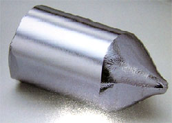
- 2 and 3 inch S-doped/ n-type semiconductor InP single crystal
- VGF growth system
- high temperature and high pressure single crystal growth furnace
- single crystal growth control system
- Advantage of InP based device
- excited wavelength match to the fiber communication (1310 ~ 1550 nm)
- high electron mobility
- high thermal conductivity
- low power loss
- low noise
Applicaiton and development of InP based device
- Optical fiber communication
- global cable laying = earth/moon distance x 8; 15 % increase/year (ref. Corning)
- urban development of FTTx; by Verizon/AT&T; @ Level 3
- long haul DWDM by fiber communication increasing: 10 Gbs →40 Gbs→160 Gbs
- Optoelectronic integration circuit
- For a faster transmission and enhanced system function, Optical-to-Optical (OEO) conversion costs of the data transmission can not be ignored as the increased of discrete components.
- cost considerations force the fiber communications components shift from a discrete component to a photonic integrated circuits (PIC)
- InP photonic integrated circuits, in recent years, getting breakthrough in the optical communications as the electronic integrated circuit technology development of Si.
- Millimeter wave in military communication
- Technology for frequency agile digitally synthesized transmitters program (DARPA, 2003), demanding the development of transistors with cut-off frequencies of up 500 GHz。
- Sub-millimeter wave imaging focal plane technology (DARPA, 2006), building an imaging system operating at 340 GHz。
- Terahertz electronics program (DARPA, 2009); Phase I: 670 GHz, Phase II: 850 GHz, Phase III: 1030 GHz。
InP based optoelectronic device industry
Table. Turnover of InP device industry in USA, 2009’ (U$)
|
Ps.
- Turnover from the number of public information
- Optical communication company chosen in USA
InP based optoelectronic device industry
- More than 150 InP based optoelectronic components manufacturers and research institutes
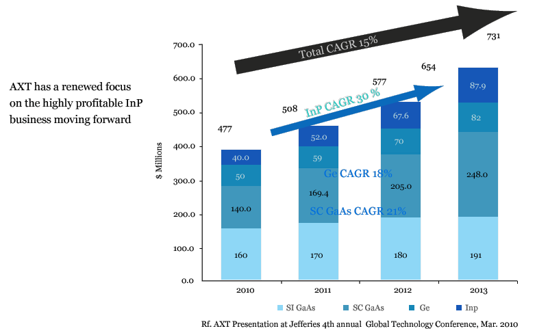
- InP based optoelectronic device market status
- sales of InP based laser and photodetectors > US$2.0 B
- market size of InP based optoelectronic device > US$5.0 B
- Similar to the GaAs, InP based optoelectronic device has grown and being mature for decades study.
- Production cost
- most important factor: lack of cheap/good InP wafer
InP wafer industry status
Only 5 global manufacturers of InP wafers
|
Nearly 80 % of the wafer supplied by Japan, and the price is expensive.
Total market opportunity
InP crystal growth process
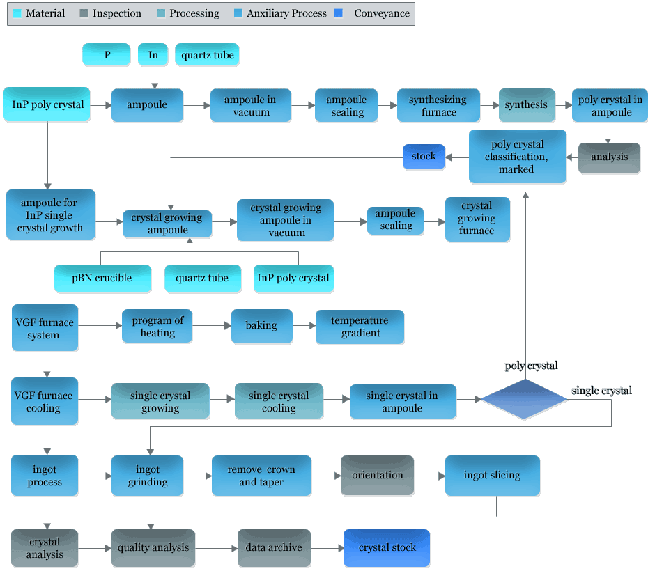
Innovation of single crystal growth technology
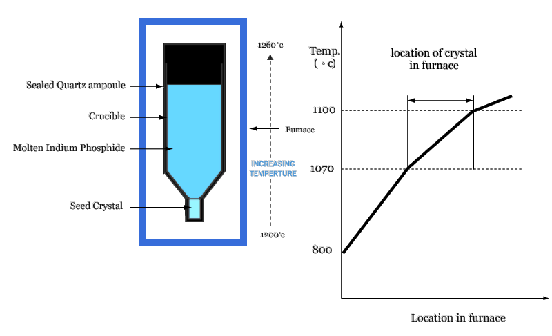
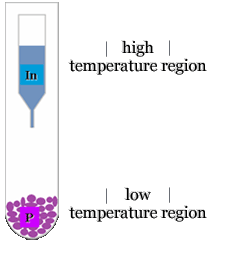
Temperature gradient in VGF
Single crystal grown by various technologies
|
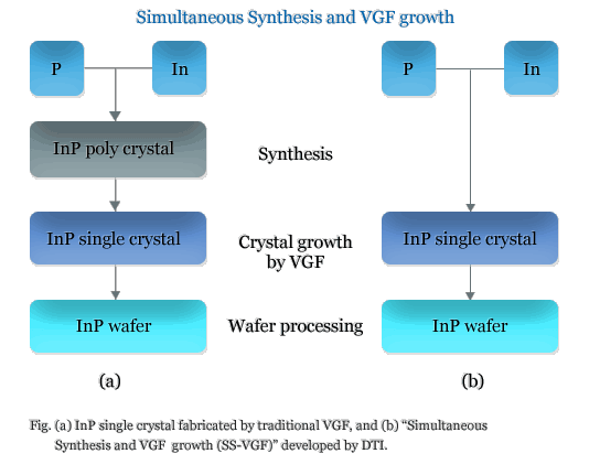
Simultaneous Synthesis and VGF growth
- Cornerstone
- key technology: VGF
- Advantage of VGF: crystal quality & yield
- Objective
- more streamlined steps
- cost down: time, equipment, space, labor…
- competitiveness: lower price product
- Difficulty
- hardware: heating element, crucible supporting design, high pressure gas flow control, temperature gradient…
- urgency: funds…
- Superiority: an expert in VGF
Comparison of InP single crystals fabricated by DTI and others
|
Main task in this project
- High temperature/high pressure furnace development
- Multiple heating system
- Crucible and supporting desing
- Thermal simulation and temperature gradient
- Crystal quality analysis
- Optoelectronic characteristics analysis
- Crystal quality control
- Process optimization of 2” S-doped InP single crystal
- Process optimization of 3” S-doped InP single crystal
(I) InP single crystal
Table . Technical specifications evolution of InP single crystal through this project
|
(II) high temperature/high pressure furnace
Table . Technical specifications evolution of high temperature/ high pressure furnace through this project
|
- Advantage of SS-VGF ® DTI
- reduce the InP single crystal growth process; diminish the facilities, space, and operator; cost down
- get high quality and low-cost products
- Hardware R & D
- high temperature/high pressure tank
- R & D capability – teamwork of materials science and engineering, electrical and electronics, mechanical engineering
- high temperature/high pressure furnace – General manager Rudy
- InP single crystal growth – Dr. Hu
- analysis and QC – Mr. Jason, Dr. Chen
- factory – Mr. Tsai
Cost Estimation
|
||||||||||||||||||||||||||||||||||||||||||||||||
|
||||||||||||||||||||||||||||||||||||||||||||||||
*A 20% of quantity of increased due to material waste during process
- Increase market value and share
- Production capacity of 2” and 3” S-doped InP single crystal > 1,000 kg/year
- Create the market value of InP wafer around U$ 8M ~ 10M (10 % of global market share), and a market value of the related laser/fiber communication device up to U$ 200M
- Intellectual property rights/ Patent
- 1 patent and 1 research paper every year
- IP: furnace, heating element, supporting of crucible, high pressure gas flow controlling, key technologies of single crystal growth