- 首頁
- 關於我們
- 商品櫥窗
- BA/EP 不銹鋼管 [12]
- 不銹鋼BA管/光輝退火管/無縫不鏽鋼管(Bright Annealed Tube / Pipe )
- 不銹鋼EP管/電解拋光管/(Stainless Steel ElectroPolished Tube / Pipe )
- 不銹鋼衛生管(BPE-TUBE)/優耐特不鏽鋼管Rath/United
- 冷鍛BA管/®DTI Cold Forged Bright Annealed Stainless Steel Tubing/不銹鋼冷鍛ba管
- 半無縫 BA 管 ( Bright Annealed Semi Seamless Stainless Steel Tube / Pipe)/BA 半無縫管
- 不鏽鋼盤管/BA/EP不銹鋼捲管/不鏽鋼捲形管/ 軟態不鏽鋼管(BA/EP Coiled Stainless Steel Tubing)
- 無縫鋼管/不銹鋼無縫管/無縫不鏽鋼管/BA管/EP管 /(®DTI Cold Forged Bright Annealed Stainless Steel Tubing/Pipe)
- 無縫管/不銹鋼無縫管/無縫不鏽鋼管(®DTI Cold Forged Bright Annealed Stainless Steel Tubing/Pipe)
- 熱交換管 (Heat Exchanger Tube)/不銹鋼換熱管/無縫熱交換管
- 精密不鏽鋼管/小口徑不銹鋼管 ( Small Diameter Stainless Steel Tube / Pipe)/Kyoto Seiken Precision Stainless Steel Tubing
- 高潔淨氣體管路/高純度氣體管線/High Purity Gas Fittings/Swagelok Parker Stainless Steel Ultra High purity Fittings
- KUZE 不銹鋼BA/EP管/電解拋光管(Stainless Steel ElectroPolished Tube / Pipe ) Kuze / Rath / United Standards
- 真空軟管 [15]
- 波紋管/不鏽鋼軟管(Stainless Steel Vacuum Bellows)/不銹鋼波紋管
- 不銹鋼軟管 ( Vacuum Flexible Hose),伸縮接頭/防震接頭
- 超級波紋管(Super Bellows)
- 無縫不鏽鋼波紋管 (Seamless Metal Bellows)
- 真空軟管(Stainless Steel KF Vacuum Bellows)
- 真空伸縮軟管(Stainless Steel ISO Vacuum Bellows)
- 不銹鋼 CF 真空軟管/真空波紋管(Stainless Steel CF Vacuum Bellows)
- 真空波紋軟管(Metal Welded Bellows)
- 鐵弗龍波紋管(Teflon Bellows)/PTFE Bellows 軟管/Teflon真空軟管/Parker
- 不鏽鋼波狀管(Corrugated Stainless Steel Tubing JWWA G119)/不鏽鋼波浪管(波紋管)
- 波紋管連軸器/不鏽鋼波紋管機械軸封(Bellows Mechanical Seal)
- 磁性流體軸封/真空磁流體機械軸封/真空旋轉導入(Ferrofluid Seals)/Vacuum Rotary Feedthrough
- 真空波紋管/液壓成型波紋管(Formed Bellows/Hydro Formed Bellows 成型波紋管)
- 伸縮接頭/伸縮管/防震軟管 Expansion Joint/Bellows Expansion Joint/Metal Hose/Stainless Steel Flexible Tubing
- 金屬軟管 / 高純度氣體金屬軟管( Convoluted Flexible Tubing / Metal Hose / Flexible Stainless Steel Hose)
- 真空零組件 [45]
- 真空軟管(Stainless Steel KF Vacuum Bellows)
- 超級波紋管(Super Bellows)
- 不銹鋼軟管 ( Vacuum Flexible Hose),伸縮接頭/防震接頭
- 真空波紋管 (Stainless Steel Vacuum Bellows)/不銹鋼波紋管
- 真空伸縮軟管/真空蛇腹管(Stainless Steel ISO Vacuum Bellows/Bellow)
- 真空波紋管/不銹鋼 CF 真空軟管(Stainless Steel CF Vacuum Bellows)
- 無縫不鏽鋼波紋管 (Seamless Metal Bellows)
- 波紋管聯軸器/不鏽鋼波紋管連軸器(Bellows Coupling)/Flexible Shaft Coupling
- 真空波紋軟管/金屬波紋管(Metal Welded Bellows)
- 鐵弗龍波紋管(Teflon Bellows)/Teflon Bellows 軟管/Teflon真空軟管/Parker
- 真空閥門(Vacuum Angle Bellows Valve)/真空角閥/Bellows Sealed Vacuum Valves
- 真空隔膜閥/膜片閥(Vacuum Diaphragm Valve)
- 真空閥/高真空閥/超高真空閥(Stainless Steel Vacuum Valves)/真空閥門
- 真空球閥/真空球塞閥(Vacuum Ball Valve)
- 真空蝶閥(Vacuum Butterfly Valve)
- 真空逆止閥(Vacuum Check Valve)
- Swagelok 管件/接頭/閥門 SWG lsf (Swagelok Valve Tube Fittings)
- 真空管件(Stainless Steel Vacuum Fittings)/ 真空零件(Vacuum Components)/真空零組件
- 真空視窗(Vacuum Sight Glass)/真空視窗玻璃(Vacuum Viewport)/真空觀測器
- CGA DISS 接頭/管件/鋼瓶接頭 Cylinder Connections/Fittings/Adapter
- 真空導入/真空導引/真空饋通(Vacuum Feedthrough)/Vacuum Rotary Feedthroughs
- 真空管件(Stainless Steel Vacuum Fittings - KF Flange)
- 真空零件/真空零組件(Vacuum Components)
- KF 真空中心圈(Stainless Steel KF Centering Ring)/Mesh Centering Ring
- 全氟化O Ring / FFKM O RINGS/ 全氟化O型環/全氟化O型橡膠圈/ Perfluoroelastomer Morisei kako/Kalrez/Parker/NOK/Chemraz/日本製O型環
- 不銹鋼 ISO 真空中心圈(Stainless Steel ISO Vacuum Centering Ring)
- 真空法蘭(Vacuum Flange)/高真空法蘭/High Vacuum Flanges
- 不銹鋼 ISO 真空法蘭襯套(ISO Flange)
- 不銹鋼 CF 真空法蘭(Stainless Steel CF Vacuum Flange)
- 真空元件 (Vacuum Components)
- 真空管件/真空管配件(Stainless Steel KF Vacuum Fittings)
- 真空管束/管夾(Vacuum Clamp)/KF Stainless Steel Vacuum Clamp/Heata Clamp
- 真空配管(NW/KF/ISO/CF/VG/VF)
- ISO 真空轉接頭(Stainless Steel ISO Tube Adaptor)
- CF 真空法蘭管件(Stainless Steel CF Flange Tubing)
- 不銹鋼 CF 真空轉接頭(Stainless Steel CF Tube Adaptor)
- VCR 管件/接頭/閥門 VCR Fittings/VCR Couplings Parker (VCR Micro Fittings)
- 金屬波紋管/蛇腹管 Metal Bellows
- 真空腔體/不銹鋼真空腔體/不鏽鋼 VACUUM CHAMBER
- 鐵氟龍管/Teflon 軟管(PTFE/PFA )/Unigasket/US Hose/Teflon 管
- 鍛造襯套/金屬法蘭管端/自動焊接法蘭襯套/管節(Auto Welding Stub End)
- 真空級定製管件Custom Vacuum Fittings/Custom Made Vacuum Fittings
- 真空閘閥 (Vacuum Gate Valves/Vacuum Bellows valves)
- 真空過濾器/ 真空阱/ 真空陷阱 Vacuum Traps/ Vacuum Foreline Traps/ Vacuum Filter
- 真空幫浦維修/真空泵浦維修 (Vacuum Pumps / Alcatel / Balzers / Dresser / Edwards / Hyvac / Kinney / Leybold / Orion / Pfeiffer / Stokes / Varian / Welch)
- 衛生管件 [18]
- 不銹鋼EP管/電解拋光管(Stainless Steel ElectroPolished Tube / Pipe ) Kuze / Rath / United Standards
- 不銹鋼BA管/光輝退火管(Stainless Steel Bright Annealed Tube / Pipe )
- 生技製藥管件(Stainless Steel Orbital Welding Fitting)
- EP管件(Electropolished Fittings)/ 電解拋光管件
- 生技製藥夾式管件(Stainless Steel Tri - Clamp Fitting)
- 生技製藥隔膜閥/不銹鋼隔膜閥(BPE Diaphragm Valve)
- 冷鍛BA管/®DTI Cold Forged Bright Annealed Stainless Steel Tubing/不銹鋼冷鍛ba管
- 半無縫 BA 管 ( Bright Annealed Semi Seamless Stainless Steel Tube / Pipe)/ Seam Integrated Tubes
- 不銹鋼衛生管(BPE-TUBE)
- BA/EP不銹鋼捲管/不鏽鋼捲形管 (BA/EP Coiled Stainless Steel Tubing)
- 熱交換管(Heat Exchanger Tube)/不銹鋼熱交換管/無縫熱交換管/換熱管
- 管帽/不銹鋼管帽/不鏽鋼端板/衛生食品級管帽 (Sanitary Weld Cap)
- 鍛造襯套/金屬法蘭管端/自動焊接法蘭襯套/管節(Auto Welding Stub End)
- 濾網墊片/濾網膠墊/Mesh Screen Gaskets/ BPE Tri-Clamp Mesh Screen Gaskets
- 衛生級定製管件Custom Sanitary Fittings/Custom Made Hygienic Fittings
- 螺蓋旋轉瓶接頭/轉瓶接頭/零件 Vent Port Assembly/Spinner Flask Accessory/Corning
- 衛生級接頭/ 衛生級夾式接頭 (Sanitary Ferrule / Hygienic Clamp Union)
- 衛生級由任接頭/ 衛生級由令接頭 (Sanitary Union / Hygienic Union)
- 食品衛生級幫浦 [9]
- 衛生食品級轉子幫浦/泵浦(Sanitary Lobe Rotor Pumps)/Sanitary Rotary Pumps/Waukesha/Nakakin
- 衛生食品級幫浦/泵浦(Sanitary Centrifugal Pumps)
- 食品衛生級螺旋幫浦/泵浦/定量幫浦(Sanitary Progressive Cavity Pumps) / Mohno Pump
- 粉末溶解機/衛生食品級粉末溶解幫浦/泵浦 Sanitary Powder Mixer Pump
- 衛生級乳化幫浦/均質泵浦/分散幫浦 /剪力泵浦(Sanitary Shear Blender Pump Fristam)
- 食品衛生級自吸式幫浦/泵浦(Sanitary Self-priming Pumps)
- 衛生級高壓離心幫浦/泵浦(Sanitary High Pressure Centrifugal Pumps)/Fristam/ C100/C114/C216/C218/C328
- 衛生食品級 Sine 幫浦/泵浦(Sanitary Masosine Pump)/Jann Shin Disco/Shin Yuung Shuhn Machinery
- NAKAKIN 衛生食品級轉子幫浦/泵浦(NAKAKIN Sanitary Lobe Rotor Pumps)/Sanitary Rotary Pumps
- 技術及設備 [30]
- 擴散焊接機/ 真空擴散接合設備/ 擴散焊接爐 Diffusion Bonding Furnaces / PVA Tepla Type
- BA爐/光輝爐/光輝退火爐/不鏽鋼光輝爐(Bright Annealing Furnace)
- 不銹鋼壓力桶/不鏽鋼壓力桶槽/衛生級桶槽 (Stainless Steel Pressure Tank/Unicontrols/Nakakin)
- 衛生食品級軟管/衛生級軟管(Sanitary Food Grade Hose)
- 衛生食品級過濾器(Cone mill Screen)/Sanitary Strainer
- 衛生級桶式過濾器/衛生級雙桶式過濾器/衛生級過濾桶 Sanitary Basket Strainer/Filter
- 無菌空氣過濾器/衛生級桶槽呼吸閥 (Aseptic Air Vent Filter) Millipore CWVT L10 01
- 殼管式熱交換器/衛生食品級殼管式熱交換器(TEMA Tubular Heat Exchanger)
- 管式熱交換器/衛生食品級管式熱交換器(Tubular Heat Exchanger)
- 板式熱交換器/衛生食品級板式熱交換器(Heat-Exchanger)/Alfa Laval/APV/GEA/Hisaka/IWAI/Sondex
- 衛生食品級軟管(Novaflex Food Grade Hose 3A)
- 不銹鋼噴球/CIP清洗球(Stainless Steel CIP Spray Ball)
- 不銹鋼人孔/衛生級桶槽人孔(Stainless Steel Manways)
- 衛生級壓力表/食品級隔膜式壓力錶/均質機壓力表/溫度錶(Sanitary Pressure Gauge/Thermometer)
- 靜態攪拌器/靜態混合器/衛生級靜態混合管(Static Mixer )/ Noritake Type
- 衛生級排氣閥 /食品級排氣閥(Sanitary Air Relief Valve)
- 法蘭襯套/不銹鋼襯套/金屬法蘭管端/ 不鏽鋼鍛造管端 (Stainless Steel Stub End / Lap Joint)
- 熱水產生器(Mixers)/蒸氣混合器
- 衛生級配管工程/自動焊接/閥串(,Orbital Welding Services & Valve Units)
- 分歧管(Manifold Tubing) /管路預製工程
- Airfloat Air Bearing /Align/氣浮軸承/空氣軸承/氣浮平台/氣浮輸送台
- 自動焊接法蘭/軌道焊接法蘭(Orbit Welding Flange/Auto Welding Flange)
- 衛生級配管/真空配管/生技配管工程/ BA/EP 配管工程
- 雷射焊接加工設備
- CIP系統(CIP/SIP)/CSF/JEC/Inoxpa/Topline
- 純蒸氣產生器(Pure Steam Generators)
- 注射水設備(WFI:Single and Multiple effect)
- 材質分析儀(Spectrum Analysis Machine)
- 锥型整粒機/粉碎整粒機 ( Cone Mill Grinder)/ Kemutec CM-1/CM-5/CM-7
- 管端加工機(Tube End Facing Machine)
- 食品衛生級閥 [22]
- 氣動隔膜閥/衛生級氣動隔膜閥(Sanitary Aseptic Pneumatic Diaphragm Valve Gemu Saunders Crane)
- 隔膜閥/生技無菌手動隔膜閥/衛生級膜片閥(Sanitary Aseptic Manual Diaphragm Gemu Saunders Crane Ohno)
- 無菌桶底隔膜閥/衛生食品級隔膜閥(Sanitary Aseptic Tank Buttom Diaphragm Valve Gemu Saunders Crane ITT)
- 三通隔膜閥/生技無菌T 型隔膜閥/衛生級膜片閥(Sanitary Aseptic 3 way Diaphragm Hygienic Gemu Saunders Crane)
- 無菌閥/無菌氣動閥(Sanitary Aseptic Valve )/F型無菌手動閥/L,T,F型 Iwai/Toyo/Izumi
- 無菌閥/無菌手動閥(Aseptic Stainless Steel Bellows Diaphragm Valve)/Iwai/Toyo/Izumi
- 衛生級氣動蝶閥(Sanitary Pneumatic Butterfly Valve Litai)
- 衛生級蝶閥(Sanitary Butterfly Valve K. Young)
- 衛生級氣動球閥(Sanitary Pneumatic Ball Valve Litai)
- 衛生級球閥(Sanitary Ball Valve)
- 衛生級氣動F型閥(Pneumatic Control F Type Divert Valve)
- 衛生級氣動L型閥(Pneumatic Control L Type Divert Valve)
- 衛生級排氣閥 /食品級排氣閥(Sanitary Air Relief Valve)
- 衛生級吹氣閥 /食品級吹氣閥(Sanitary Air Blow Valve)
- 取樣閥/無菌取樣閥/衛生級隔膜閥(Sanitary Aseptic Sample Valve )
- 充填閥/衛生級充填閥 /食品級充填閥(Sanitary Heishin Filling Valve) FV2/FV3
- 波紋管閥/無菌波紋管閥 Sanitary Bellows Valve (Ohno/Iwai/Izumi)
- Aseptic Bellows Diaphragm Valve
- 大口徑衛生級隔膜閥 Large Diameter Hygienic Diaphragm Valve
- 衛生級減壓閥/衛生級洩壓閥/衛生級安全閥 Hygienic Relief Valve/Sanitary Safety Valve/Pressure Relief Valve/Goetze/Niezgodka
- 衛生級取樣閥/無菌取樣閥 Aseptic Sampling Valve/Hygienic Sampling Valve/Bio-Components/Bioengineering/B.Braun/NBS
- 衛生級防混閥/衛生級雙座閥/衛生級防混雙座閥 ( Sanitary Mix Proof Double Seat Valve)
- 磷化銦晶圓( InP Wafer) [9]
- 磷化銦晶圓(晶片)
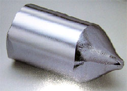
- InP 基板/磷化銦基板(單晶棒)
- InP 多晶錠/磷化銦多晶棒
- GaAs 基板/砷化鎵晶圓/晶片 (GaAs wafers)
- GaAs 基板/GaAs Substrate
- VGF 長晶爐 / 單晶生長爐(VGF Crystal Growth Furnace)
- InP Crystal Growth Simulation
- PBN 坩鍋/坩埚 Crucible/熱解氮化硼 坩鍋( Pyrolytic Boron Nitride Crucible)
- 氧化鋁基板/陶瓷基板 ( Alumina Substrate/Aluminum Oxide Al2O3 Ceramic Substrate)
- 真空管件/真空閥門 [12]
- 真空法蘭(Vacuum Flange)/高真空法蘭/High Vacuum Flanges
- 真空接頭 / 真空快速接頭 / 真空旋轉接頭 (Vacuum Quick Disconnect / Vacuum Gauge Seal Port / Vacuum Quick Connect)
- 真空破壞閥 / 破真空閥 / 真空破壞器 (Up To Air Valve / Vacuum Breaker Valve / Vacuum Leak Port)
- 真空轉接頭 / 真空法蘭轉接頭 (Vacuum Hybrid Adapter / Vacuum fitting To Flanges)
- 高純度氣體配管/氣體管路定製(Gas Delivery Product / High Purity Gas Delivery Tube Assembly)
- 不鏽鋼真空管夾 (Vacuum Stainless Steel Clamp) / KF Hinged Clamp/Bulkhead Clamps)
- 森清化工O型環/O型橡膠圈/ Morisei Kako O Ring /Kalrez/Parker/NOK/Chemraz/日本製O型環
- 真空閥門(Vacuum Angle Bellows Valve)/真空角閥/Bellows Sealed Vacuum Valves
- 真空球閥/真空球塞閥(Vacuum Ball Valves)
- 真空隔膜閥/膜片閥(Vacuum Diaphragm Valves)
- 真空蝶閥(Vacuum Butterfly Valves)
- 真空閥 / 高真空閥 / 超高真空閥(High Vacuum Valves)/真空閥門
- BA/EP 不銹鋼管 [12]
- 服務
- 新聞
- 技術
- 製程
- 磷化銦晶圓
- 聯絡我們
磷化銦晶圓
- Product Development
- Market Status
- Source of Technology
- Technical Specifications
- Competitive Analysis
- Expected Benefits
- 2 and 3 inch S-doped/ n-type semiconductor InP single crystal
- VGF growth system
- high temperature and high pressure single crystal growth furnace
- single crystal growth control system
- Advantage of InP based device
- excited wavelength match to the fiber communication (1310 ~ 1550 nm)
- high electron mobility
- high thermal conductivity
- low power loss
- low noise
Applicaiton and development of InP based device
- Optical fiber communication
- global cable laying = earth/moon distance x 8; 15 % increase/year (ref. Corning)
- urban development of FTTx; by Verizon/AT&T; @ Level 3
- long haul DWDM by fiber communication increasing: 10 Gbs →40 Gbs→160 Gbs
- Optoelectronic integration circuit
- For a faster transmission and enhanced system function, Optical-to-Optical (OEO) conversion costs of the data transmission can not be ignored as the increased of discrete components.
- cost considerations force the fiber communications components shift from a discrete component to a photonic integrated circuits (PIC)
- InP photonic integrated circuits, in recent years, getting breakthrough in the optical communications as the electronic integrated circuit technology development of Si.
- Millimeter wave in military communication
- Technology for frequency agile digitally synthesized transmitters program (DARPA, 2003), demanding the development of transistors with cut-off frequencies of up 500 GHz。
- Sub-millimeter wave imaging focal plane technology (DARPA, 2006), building an imaging system operating at 340 GHz。
- Terahertz electronics program (DARPA, 2009); Phase I: 670 GHz, Phase II: 850 GHz, Phase III: 1030 GHz。
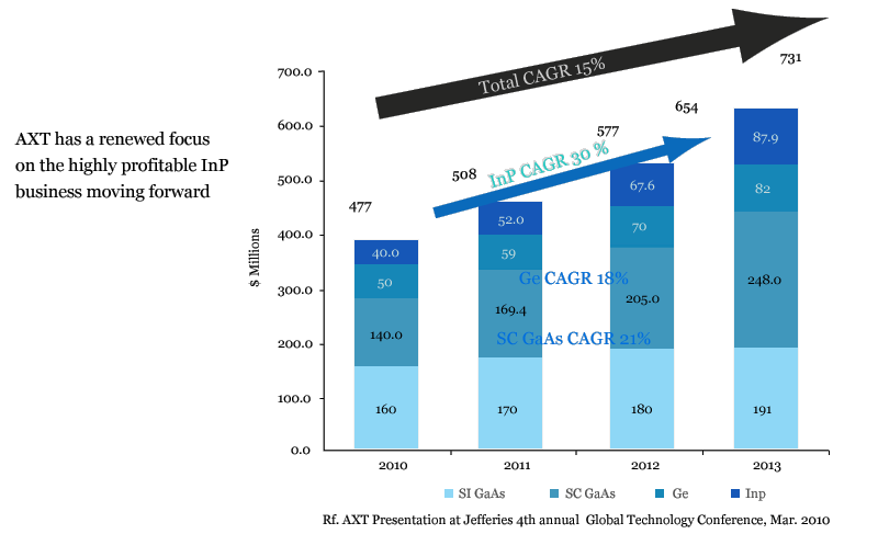
InP based optoelectronic device industry
Table. Turnover of InP device industry in USA, 2009’ (U$)
|
Ps.
- Turnover from the number of public information
- Optical communication company chosen in USA
InP based optoelectronic device industry
- More than 150 InP based optoelectronic components manufacturers and research institutes
- InP based optoelectronic device market status
- sales of InP based laser and photodetectors > US$2.0 B
- market size of InP based optoelectronic device > US$5.0 B
- Similar to the GaAs, InP based optoelectronic device has grown and being mature for decades study.
- Production cost
- most important factor: lack of cheap/good InP wafer
InP wafer industry status
Only 5 global manufacturers of InP wafers
|
Nearly 80 % of the wafer supplied by Japan, and the price is expensive.
Total market opportunity
InP crystal growth process
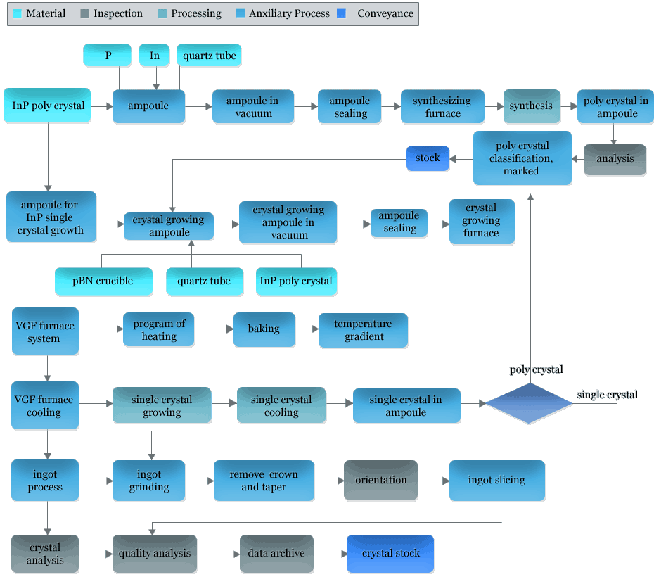
Innovation of single crystal growth technology
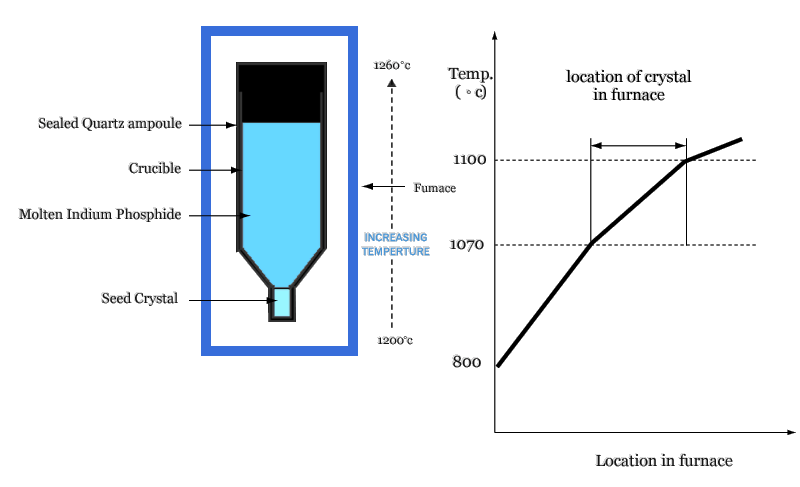
Temperature gradient in VGF
Single crystal grown by various technologies
|
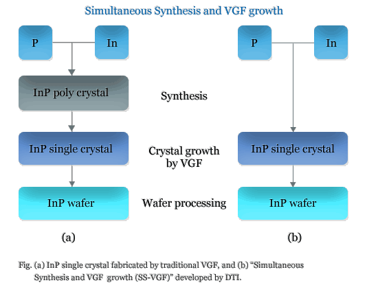
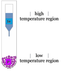
Simultaneous Synthesis and VGF growth
- Cornerstone
- key technology: VGF
- Advantage of VGF: crystal quality & yield
- Objective
- more streamlined steps
- cost down: time, equipment, space, labor…
- competitiveness: lower price product
- Difficulty
- hardware: heating element, crucible supporting design, high pressure gas flow control, temperature gradient…
- urgency: funds…
- Superiority: an expert in VGF
Comparison of InP single crystals fabricated by DTI and others
|
Main task in this project
- High temperature/high pressure furnace development
- Multiple heating system
- Crucible and supporting desing
- Thermal simulation and temperature gradient
- Crystal quality analysis
- Optoelectronic characteristics analysis
- Crystal quality control
- Process optimization of 2” S-doped InP single crystal
- Process optimization of 3” S-doped InP single crystal
(I) InP single crystal
Table . Technical specifications evolution of InP single crystal through this project
|
(II) high temperature/high pressure furnace
Table . Technical specifications evolution of high temperature/ high pressure furnace through this project
|
- Advantage of SS-VGF ® DTI
- reduce the InP single crystal growth process; diminish the facilities, space, and operator; cost down
- get high quality and low-cost products
- Hardware R & D
- high temperature/high pressure tank
- R & D capability – teamwork of materials science and engineering, electrical and electronics, mechanical engineering
- high temperature/high pressure furnace – General manager Rudy
- InP single crystal growth – Dr. Hu
- analysis and QC – Mr. Jason, Dr. Chen
- factory – Mr. Tsai
Cost Estimation
|
||||||||||||||||||||||||||||||||||||||||||||||||
|
||||||||||||||||||||||||||||||||||||||||||||||||
*A 20% of quantity of increased due to material waste during process
- Increase market value and share
- Production capacity of 2” and 3” S-doped InP single crystal > 1,000 kg/year
- Create the market value of InP wafer around U$ 8M ~ 10M (10 % of global market share), and a market value of the related laser/fiber communication device up to U$ 200M
- Intellectual property rights/ Patent
- 1 patent and 1 research paper every year
- IP: furnace, heating element, supporting of crucible, high pressure gas flow controlling, key technologies of single crystal growth