- 首页
- 关于我们
- 商品橱窗
- BA/EP 不锈钢管 [13]
- 不锈钢BA管, 不锈钢光辉退火管, 无缝不锈钢管(Bright Annealed Tube / Pipe )
- 不锈钢EP管, 不锈钢电解抛光管 (Stainless Steel ElectroPolished Tube / Pipe )
- 卫生级不锈钢管, 食品级不锈钢管, 优耐特不锈钢管Rath/United
- 不锈钢冷锻BA管, 无缝不锈钢精密管 有缝不锈钢精抽管, ®DTI Cold Forged Bright Annealed Stainless Steel Tubing/不锈钢冷锻ba管
- 半无缝 BA 管 ( Bright Annealed Semi Seamless Stainless Steel Tube / Pipe)/BA 半无缝管
- 不锈钢盘管, BA/EP不锈钢卷管, 不锈钢卷形管, 软态不锈钢管(BA/EP Coiled Stainless Steel Tubing), Level Wound Coil Stainless Steel Tube, KUZE / Handy Tube Standard
- 无缝钢管, 不锈钢无缝管, 无缝不锈钢管, BA管, EP管(®DTI Cold Forged Bright Annealed Stainless Steel Tubing/Pipe)
- 无缝管, 不锈钢无缝管, 无缝不锈钢管(®DTI Cold Forged Bright Annealed Stainless Steel Tubing/Pipe)
- 热交换管 (Heat Exchanger Tube), 不锈钢换热管, 不锈钢无缝热交换管
- 精密不锈钢管, 小口径不锈钢管 ( Small Diameter Stainless Steel Tube / Pipe) / Teshima /Kyoto Seiken Precision Stainless Steel Tubing
- 高洁净气体管路,/ 高纯度气体管线, High Purity Gas Fittings/Swagelok Parker Stainless Steel Ultra High purity Fittings
- KUZE 不锈钢BA/EP管, 电解抛光管(Stainless Steel ElectroPolished Tube / Pipe ) Kuze / Rath / United Standards
- 气压缸不锈钢管,精密冷抽不锈钢气压缸管 (Pneumatic Cylinder Stainless Steel Tube, Air Cylinder Tube/ Pipe)
- 真空波纹管/真空软管 [21]
- 真空波纹管, 不锈钢真空软管(Stainless Steel Vacuum Bellows) / 不锈钢波纹管
- 不锈钢软管, 不锈钢伸缩接头, 不锈钢防震接头
- 超级波纹管, 不锈钢超级波纹管 (Super Bellows)
- 无缝不锈钢波纹管 (Seamless Metal Bellows)
- 真空软管, 真空波纹管 (Stainless Steel KF Vacuum Bellows)
- ISO真空软管, ISO真空伸缩软管(Stainless Steel ISO Vacuum Bellows)
- CF 真空软管, 不锈钢真空波纹管(Stainless Steel CF Vacuum Bellows)
- 焊接波纹管, 焊接式波纹管, 真空波纹软管(Metal Welded Bellows)
- 铁弗龙波纹管(Teflon Bellows), PTFE Bellows真空软管, Teflon真空软管/ Parker
- 不锈钢波状管(Corrugated Stainless Steel Tubing JWWA G119)/不锈钢波浪管(波纹管)
- 波纹管连轴器, 不锈钢波纹管联轴器, 不锈钢波纹管机械轴封(Bellows Mechanical Seal)
- 磁流体轴封, 磁性流体轴封, 真空磁流体机械轴封, 真空旋转导入(Ferrofluid Seals)/Vacuum Rotary Feedthrough
- 真空波纹管, 液压成型波纹管(Formed Bellows/Hydro Formed Bellows 成型波纹管)
- 真空伸缩接头, 真空伸缩管, 防震软管 Expansion Joint/Bellows Expansion Joint/Metal Hose/Stainless Steel Flexible Tubing
- 小口径不锈钢软管, 小口径真空波纹管, 高纯度气体不锈钢软管( Convoluted Flexible Tubing / Metal Hose / Flexible Stainless Steel Hose)
- 焊接波纹管, 焊接式波纹管, 边缘焊接式波纹管, Edge Welded Bellows / Vacuum Bellows/ Mewasa Type
- 消防软管, 消防撒水软管, 不锈钢消防洒水软管(Flexible Sprinkler Hose)
- 涡轮增压器排油管,不锈钢涡轮回油管, Turbo Charger Oil Drain Tube, Detroit Diesel Turbo Charger Oil Drain Pipe, Detroit Diesel Flex Stainless Steel Pipe
- 废气再循环管, 不锈钢EGR 管, Exhaust Gas Recirculation Tube, EGR Tube, EGR pipe
- 空气喷射歧管,不锈钢空气喷射歧管,二次空气喷射反应管, Secondary Air Injection Tube, AI Tube, Air Tube
- 不锈钢涡轮供油管,Turbo Oil Feed Tube, Turbo Charger Oil Feed Line, Detroit Diesel Flex Stainless Steel Pipe,
- 真空零组件 [50]
- 真空软管, 真空压缩软管(Stainless Steel KF Vacuum Bellows)
- 超级波纹管(Super Bellows)
- 不锈钢软管, 不锈钢伸缩接头, 不锈钢防震接头
- 真空波纹管 (Stainless Steel Vacuum Bellows), 不锈钢波纹管
- ISO真空波纹管, 真空伸缩软管, 真空蛇腹管(Stainless Steel ISO Vacuum Bellows/Bellow)
- 真空波纹管/ 不锈钢 CF 真空软管(Stainless Steel CF Vacuum Bellows)
- 无缝不锈钢波纹管 (Seamless Metal Bellows)
- 波纹管联轴器, 不锈钢波纹管连轴器(Bellows Coupling), Flexible Shaft Coupling
- 焊接波纹管, 焊接型波纹管, 边缘焊接波纹管, 真空波纹软管, 金属波纹管(Metal Welded Bellows)
- 铁弗龙波纹管(Teflon Bellows), Teflon Bellows 软管, Teflon真空软管/ Parker
- 真空角阀(Vacuum Angle Bellows Valve), 真空阀门(Bellows Sealed Vacuum Valves)
- 真空隔膜阀, 真空膜片阀(Vacuum Diaphragm Valve)
- 真空阀, 高真空阀, 超高真空阀(Stainless Steel Vacuum Valves)/真空阀门
- 真空球阀, 真空球塞阀(Vacuum Ball Valve)
- 真空蝶阀(Vacuum Butterfly Valve)
- 真空逆止阀, 真空止回阀, 不锈钢真空逆止阀 (Vacuum Check Valve)
- Swagelok 管件, Swagelok接头, Swagelok阀门 SWG lsf (Swagelok Valve Tube Fittings)
- 真空管件(Stainless Steel Vacuum Fittings), 真空零件(Vacuum Components), 真空零组件
- 真空视窗(Vacuum Sight Glass), 真空视窗玻璃(Vacuum Viewport)/真空观测器
- CGA DISS 接头, 钢瓶管件, 钢瓶接头 Cylinder Connections/Fittings/Adapter
- 真空导入, 真空导引, 真空馈通(Vacuum Feedthrough)/Vacuum Rotary Feedthroughs
- 真空管件(Stainless Steel Vacuum Fittings - KF Flange)
- 真空零件, 真空零组件 (Vacuum Components)
- KF 真空中心圈(KF Centering ), 滤网中心圈(Mesh Centering)
- 全氟化O Ring, FFKM O RINGS, 全氟化O型环, 全氟化O型橡胶圈, Perfluoroelastomer Morisei kako/Kalrez/Parker/NOK/Chemraz/日本制O型环
- ISO中心圈, 不锈钢 ISO 真空中心圈(Stainless Steel ISO Vacuum Centering Ring)
- 真空法兰, 高真空法兰, CF真空法兰 (High Vacuum Flanges)
- ISO真空法兰, 不锈钢 ISO 真空法兰衬套(ISO Vacuum Flange)
- 不锈钢 CF 真空法兰(Stainless Steel CF Vacuum Flange)
- 真空元件 (Vacuum Components)
- 真空管件, 真空管配件(Stainless Steel KF Vacuum Fittings)
- 真空管束, 真空管夹/ (Vacuum Clamp)/ KF Stainless Steel Vacuum Clamp/Heata Clamp
- 真空配管, 真空管路, 真空配管规格 (NW/KF/ISO/CF/VG/VF)
- ISO 真空转接头(Stainless Steel ISO Tube Adaptor)
- CF 真空法兰管件(Stainless Steel CF Flange Tubing)
- 不锈钢 CF 真空转接头(Stainless Steel CF Tube Adaptor)
- VCR 管件, VCR接头, VCR阀门, 气体管件 ( VCR Fittings / VCR Couplings Parker / VCR Micro Fittings)
- 金属波纹管, 真空蛇腹管 Metal Bellows
- 真空腔体, 不锈钢真空腔体, 不锈钢 VACUUM CHAMBER
- 食品级软管, 铁氟龙管, Teflon 软管(PTFE/PFA )/ Unigasket/ US Hose/ Teflon 管
- 锻造衬套, 金属法兰管端, 自动焊接法兰衬套/管节(Auto Welding Stub End)
- 客制化真空管件, 真空级订制管件,真空预制管道 (Custom Vacuum Fittings), Custom Made Vacuum Fittings
- 真空闸阀, 真空插板阀 (Vacuum Gate Valves/Vacuum Bellows valves)
- 真空过滤器, 真空阱, 真空陷阱 (Vacuum Traps/ Vacuum Foreline Traps/ Vacuum Filter)
- 真空帮浦维修, 真空泵浦配管零件 (Vacuum Pumps / Alcatel / Balzers / Dresser / Edwards / Hyvac / Kinney / Leybold / Orion / Pfeiffer / Stokes / Varian / Welch)
- KF真空法兰,高真空法兰 (KF Vacuum Flanges)
- VG真空法兰,VF真空法兰,高真空法兰 (VG/VF Vacuum Flanges)
- 三菱O型环, 密封圈, 垫片(MITSUBISHI SEAL, PACKING, GASKET, O Ring / Kalrez/ Parker/ NOK/Chemraz/ 日本制O型环
- NICHIAS垫片,TOMBO 垫片, Gaskets, Packing, O Rings, PTFE垫片, TEFLON垫片, FFKM O RINGS, 全氟化O型环, 全氟化O型橡胶圈
- 真空消音器,真空帮浦消音器,真空泵消音器 ,Vacuum Silencer, Vacuum Exhaust Silencer, Vacuum Pump Silencer, Edwards Standard
- 卫生级管件 [19]
- 不锈钢EP管, 不锈钢电解抛光管(Stainless Steel ElectroPolished Tube / Pipe ) Kuze / Rath / United Standards
- 不锈钢BA管, 不锈钢光辉退火管(Stainless Steel Bright Annealed Tube / Pipe )
- 生技制药管件(Stainless Steel Orbital Welding Fitting)
- EP管件(Electropolished Fittings), 电解抛光管件
- 生技制药夹式管件(Stainless Steel Tri - Clamp Fitting)
- 卫生级隔膜阀, 生技制药隔膜阀, 不锈钢隔膜阀(BPE Diaphragm Valve Ohno)
- 冷锻BA管, ®DTI Cold Forged Bright Annealed Stainless Steel Tubing, 不锈钢冷锻ba管
- 半无缝 BA 管 ( Bright Annealed Semi Seamless Stainless Steel Tube / Pipe)/ Seam Integrated Tubes
- 卫生级不锈钢管, 不锈钢卫生管(BPE-TUBE)
- BA/EP不锈钢卷管, 不锈钢卷形管 (BA/EP Coiled Stainless Steel Tubing)
- 不锈钢热交换管(Heat Exchanger Tube), 不锈钢热交换管, 无缝热交换管, 换热管
- 卫生级管帽, 不锈钢管帽, 不锈钢端板, 食品级管帽 (Sanitary Weld Cap)
- 锻造衬套, 金属法兰管端, 自动焊接法兰衬套/管节(Auto Welding Stub End)
- 卫生级滤网垫片, 食品级滤网胶垫/Mesh Screen Gaskets/ BPE Tri-Clamp Mesh Screen Gaskets
- 客制化卫生级管件, 卫生级订制管件,卫生级预制管路 (Custom Sanitary Fittings), Custom Made Hygienic Fittings
- 螺盖旋转瓶接头, 转瓶接头/零件 Vent Port Assembly/Spinner Flask Accessory/Corning
- 卫生级接头, 卫生级夹式接头 (Sanitary Ferrule / Hygienic Clamp Union)
- 卫生级由任接头, 卫生级由令接头 (Sanitary Union / Hygienic Union)
- 双扣式快速接头,双臂式快速接头,不锈钢大流量快速接头 (Camlock Couplings, Pixon Camlock Fittings, Camlock Quick Disconnect Couplings)
- 食品卫生级帮浦 [11]
- 卫生食品级转子帮浦, 卫生级转子泵浦(Sanitary Lobe Rotor Pumps)/Sanitary Rotary Pumps/Waukesha/Nakakin
- 卫生级泵浦, 卫生级离心泵浦 (Osaka Sanitary Centrifugal Pumps Types)
- 食品卫生级螺旋帮浦, 高黏度泵浦, 定量帮浦(Sanitary Progressive Cavity Pumps) / Mohno Pump
- 粉末溶解机, 卫生级粉末溶解帮浦, 食品级粉末溶解泵浦 ( Sanitary Powder Mixer Pump)
- 卫生级乳化帮浦, 食品级均质泵浦, 分散帮浦, 剪力泵浦(Sanitary Shear Blender Pump Fristam)
- 食品卫生级自吸式帮浦/泵浦(Iwai Kikai Kogyo Sanitary Self-priming Pumps Type)
- 卫生级高压离心帮浦, 卫生级离心泵浦(Sanitary High Pressure Centrifugal Pumps)/Fristam/ C100/C114/C216/C218/C328/CSF
- 食品级 Sine 帮浦, 卫生级泵浦(Sanitary Masosine Pump)/Jann Shin Disco/Shin Yuung Shuhn Machinery
- NAKAKIN 卫生食品级转子帮浦/泵浦(NAKAKIN Sanitary Lobe Rotor Pumps)/Sanitary Rotary Pumps
- Waukesha 卫生食品级转子帮浦/泵浦(Waukesha Sanitary Lobe Rotor Pumps)/Sanitary Rotary Pumps
- Osaka 卫生级离心帮浦, 卫生级泵浦(Osaka Sanitary Centrifugal Pumps) SE
- 工程及设备 [32]
- 卫生级过滤器, 食品级过滤器(Cone mill Screen)/Sanitary Strainer
- 卫生级桶式过滤器, 卫生级双桶式过滤器, 卫生级过滤桶 (Sanitary Basket Strainer/Filter )
- 扩散焊接机, 扩散焊接代工, 真空扩散接合设备, 扩散焊接炉 Diffusion Bonding Furnaces / PVA Tepla Type
- 不锈钢压力桶, 不锈钢加压容器, 不锈钢保压桶, 卫生级桶槽 (Stainless Steel Pressure Tank / Unicontrols / Nakakin)
- 卫生级软管, 食品级软管(Sanitary Food Grade Hose)
- 无菌空气过滤器, 卫生级桶槽呼吸阀 (Aseptic Air Vent Filter) Millipore CWVT L10 01
- 卫生级壳管式热交换器, 食品级壳管式热交换器(TEMA Tubular Heat Exchanger)
- 卫生级管式热交换器, 卫生食品级管式热交换器(Tubular Heat Exchanger)
- 板式热交换器, 卫生食品级板式热交换器(Heat-Exchanger)/Alfa Laval/APV/GEA/Hisaka/IWAI/Sondex
- 食品级软管,卫生食品级软管(Novaflex Food Grade Hose 3A Toyox )
- 卫生级喷球, 不锈钢喷球, CIP清洗球(Stainless Steel CIP Spray Ball)
- 不锈钢人孔, 卫生级桶槽人孔(Stainless Steel Manways)
- 卫生级压力表, 食品级隔膜式压力表, 均质机压力表, 卫生级温度表(Sanitary Pressure Gauge/Thermometer)
- 静态混合器, 静态混合管, 食品级静态混合器, 卫生级静态混合管(Static Mixer )/ Noritake Type
- 卫生级排气阀, 食品级排气阀(Sanitary Air Relief Valve)
- 法兰衬套, 不锈钢衬套, 金属法兰管端, 不锈钢锻造管端 (Stainless Steel Stub End / Lap Joint)
- 热水产生器(Mixers), 蒸气混合器
- 不锈钢筛网, 不锈钢标准筛网 (Test Stainless Steel Sieving)
- 卫生级配管工程, 自动焊接, 阀串(,Orbital Welding Services & Valve Units)
- 分歧管(Manifold Tubing), 管路预制工程
- Airfloat Air Bearing / Align, 气浮轴承, 空气轴承, 气浮平台/ 气浮输送台
- 自动焊接法兰, 轨道焊接法兰(Orbit Welding Flange/Auto Welding Flange)
- 卫生级配管, 真空配管, 生技配管工程, BA/EP 配管工程
- 雷射焊接加工设备
- BA炉, 光辉炉, 光辉退火炉, 不锈钢光辉炉(Bright Annealing Furnace)
- CIP系统(CIP/SIP), CSF, JEC, Inoxpa, Topline
- 纯蒸气产生器(Pure Steam Generators)
- 注射水设备(WFI:Single and Multiple effect)
- 材质分析仪(Spectrum Analysis Machine)
- 锥型整粒机, 粉碎整粒机 ( Cone Mill Grinder)/ Kemutec CM-1/CM-5/CM-7
- 管端加工机(Tube End Facing Machine)
- Alfagomma 软管, Alfagomma 工业软管/橡胶软管 (Alfagomma Rubber Hose FDA)
- 食品卫生级阀门 [27]
- 卫生级气动隔膜阀, 食品级气动隔膜阀(Sanitary Aseptic Pneumatic Diaphragm Valve Gemu Saunders Crane)
- 卫生级隔膜阀, 生技无菌手动隔膜阀, 卫生级膜片阀(Sanitary Aseptic Manual Diaphragm Gemu Saunders Crane Ohno)
- 无菌桶底隔膜阀, 卫生食品级桶底隔膜阀(Sanitary Aseptic Tank Buttom Diaphragm Valve Gemu Saunders Crane ITT)
- 卫生级三通隔膜阀, 生技无菌T 型隔膜阀, 卫生级膜片阀(Sanitary Aseptic 3 way Diaphragm Hygienic Gemu Saunders Crane)
- 无菌阀, 无菌气动阀(Sanitary Aseptic Valve ) , F型无菌手动阀/L,T,F型 Iwai/Toyo/Izumi
- 卫生级无菌阀, 无菌手动阀(Aseptic Stainless Steel Bellows Diaphragm Valve)/Iwai/Toyo/Izumi
- 卫生级气动蝶阀(Sanitary Pneumatic Butterfly Valve Litai)
- 卫生级蝶阀(Sanitary Butterfly Valve K. Young)
- 卫生级气动球阀(Sanitary Pneumatic Ball Valve Litai)
- 卫生级球阀, 食品级球阀 (Sanitary Ball Valve)
- 卫生级气动F型阀(Osaka Sanitary Type Pneumatic Control F Type Divert Valve)
- 卫生级气动L型阀(Pneumatic Control L Type Divert Valve)
- 卫生级排气阀, 食品级排气阀(Sanitary Air Relief Valve)
- 卫生级吹气阀, 食品级吹气阀(Sanitary Air Blow Valve)
- 卫生级取样阀, 无菌取样阀, 卫生级隔膜阀(Sanitary Aseptic Sample Valve )
- 卫生级充填阀, 食品级充填阀(Sanitary Heishin Filling Valve) FV2/FV3
- 卫生级波纹管阀, 无菌波纹管阀 Sanitary Bellows Valve (Ohno/Iwai/Izumi)
- 卫生级波纹管阀门 (Aseptic Bellows Diaphragm Valve)
- 大口径卫生级隔膜阀, 大尺寸卫生级隔膜阀 ( Large Diameter Hygienic Diaphragm Valve)
- 卫生级减压阀, 卫生级调压阀, 卫生级安全阀 Hygienic Relief Valve/Sanitary Safety Valve/Pressure Relief Valve/Goetze/Niezgodka
- 卫生级取样阀, 无菌取样阀 (Aseptic Sampling Valve/Hygienic Sampling Valve/Bio-Components/Bioengineering/B.Braun/NBS)
- 卫生级防混阀, 卫生级双座阀, 卫生级防混双座阀 ( Sanitary Mix Proof Double Seat Valve)
- 大口径卫生级蝶阀, 大尺寸食品级蝶阀 ( Large Diameter Hygienic Butterfly Valve )
- Osaka 卫生级球阀, 食品级球阀 (Osaka Sanitary Ball Valve)
- Osaka/ Top Line 卫生级考克阀,食品级考克阀,卫生级旋塞阀 (Osaka/ Top Line Sanitary Plug Valve)
- 卫生级逆止阀,卫生级止回阀,不锈钢食品级逆止阀 (Sanitary Check Valve)
- Osaka 卫生级气动阀, 食品级气动阀 (Osaka Sanitary Pneumatic Valve)
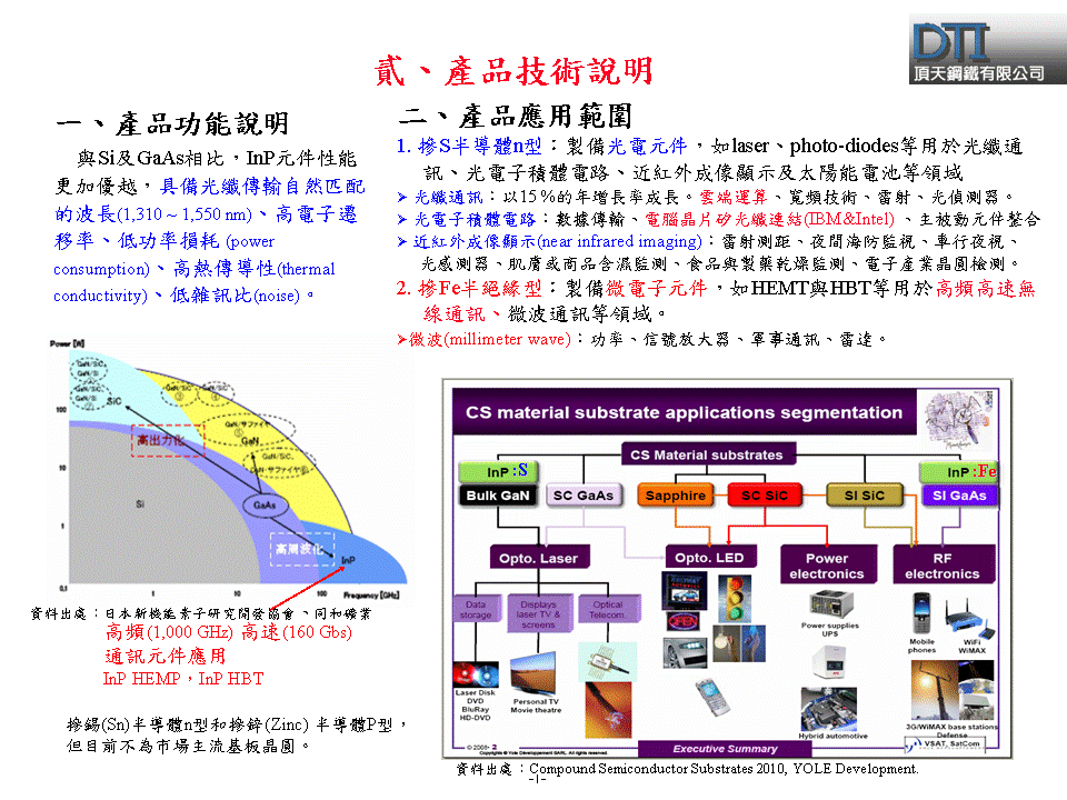
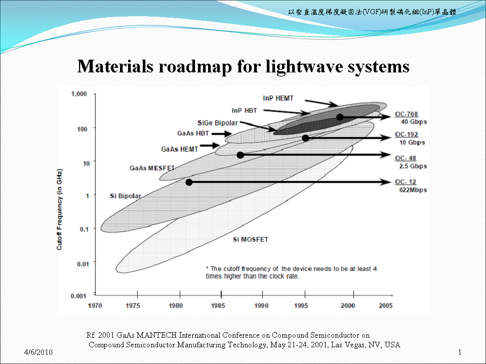
- 磷化铟晶圆( InP Wafer) [9]
- 真空管件/真空阀门 [16]
- 真空法兰, 高真空法兰, CF真空法兰 (High Vacuum Flanges)
- 真空接头, 真空快速接头, 真空旋转接头 (Vacuum Quick Disconnect / Vacuum Gauge Seal Port / Vacuum Quick Connect)
- 真空破坏阀, 破真空阀, 真空破坏器 (Up To Air Valve / Vacuum Breaker Valve / Vacuum Leak Port)
- 真空转接头, 真空法兰转接头, 真空配管转接头 (Vacuum Hybrid Adapter / Vacuum fitting To Flanges)
- 高纯度气体配管, 气体管路定制(Gas Delivery Product / High Purity Gas Delivery Tube Assembly)
- 不锈钢真空管夹, 不锈钢真空管束 (Vacuum Stainless Steel Clamp) / KF Hinged Clamp/Bulkhead Clamps)
- 森清化工O-Ring,森清化工 O型环, 日本O型橡胶圈, Morisei Kako O Ring /Kalrez/Parker/NOK/Chemraz/日本制O型环
- 真空阀门, 真空阀件, 真空角阀, 真空闸阀 (Vacuum Bellows Valve)
- 真空球阀, 真空球塞阀(Vacuum Ball Valves)
- 真空隔膜阀, 真空膜片阀, 真空隔膜调压阀 (Vacuum Diaphragm Valves)
- 真空蝶阀 (Vacuum Butterfly Valves)
- 真空阀, 高真空阀, 超高真空阀, 真空气动阀
- 地板阀, 真空墙阀, 吸尘插座(Vacuum Floor Inlet Valves)
- 焊接波纹管, 焊接式波纹管, 边缘焊接式波纹管, Edge Welded Bellows / Vacuum Bellows/ Mewasa Type
- 真空气动阀, 真空自动阀(Vacuum Electro Pneumatic Valve)
- 电磁不锈钢,日本磁性不锈钢,电磁阀铁芯材料,软磁合金 (Tohoku Steel Electromagnetic Stainless Steel)
- BA/EP 不锈钢管 [13]
- 服务
- 新闻
- 技术
- 制程
- 磷化铟晶圆
- 联系我们
商品
磷化铟晶圆(芯片)
商品型号: InP Wafer
- Indium Phosphide and Related Materials-1
- Indium Phosphide and Related Materials-2
*Wafer Specifications&Test Report
联亚光电 EPI Test Report

|
认证:
- SEMI/EJMA
订购资讯:
- 最小订购量: Negotiable
- 自行开发商品